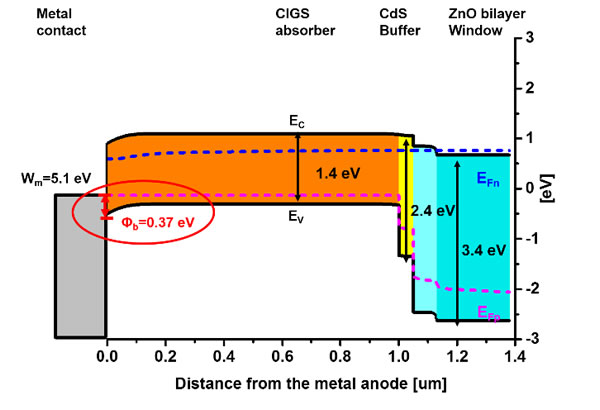
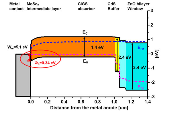
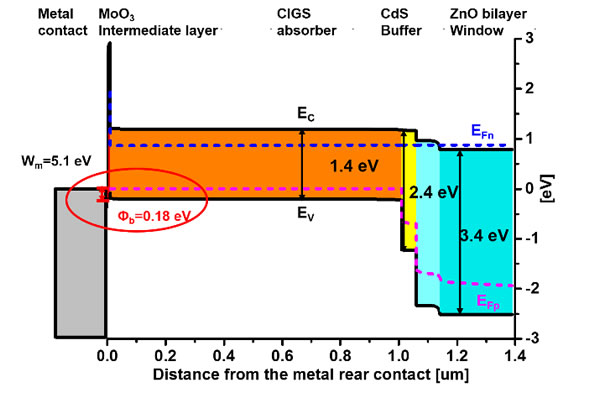
On January 15, Li Weimin, Ph.D. of the Photonic Information and Energy Materials Research Center of the Institute of Integration, Shenzhen Institute of Advanced Technology, Chinese Academy of Sciences and his research team made new progress in the field of wide band gap copper indium gallium selenide (CIGS) thin-film solar cells. The team used the method of one-dimensional solar cell capacitance simulation software (SCAPS-1D) to successfully reveal the effect of back-contact Schottky barrier and back-contact interface carrier recombination on battery performance in wide-bandgap CIGS thin-film solar cells. It also proposes a solution that uses a wide band gap MoO3 ultra-thin interlayer to effectively reduce the back contact Schottky barrier and Al2O3 passivation layer to reduce interface carrier recombination, thereby improving battery performance. Related research results were published on Solar Energy ("Solar Energy") with the title "Back Contact Interface of High Efficiency Wide Bandgap CIGS Thin Film Solar Cells" The first author of the paper is Li Weimin, and the corresponding author is researcher Yang Chunlei. CIGS thin-film solar cells are one of the most commercially promising thin-film solar cells. Currently, the band gap of high-efficiency CIGS solar cells is generally less than 1.2 eV. The benefits of increasing the CIGS band gap to 1.3 eV or more are: (1) reducing the consumption of In elements in thin-film modules by 60-70%; (2) the wide band gap CIGS cells are more compatible with the solar spectrum, and can be Obtain higher efficiency battery; (3) Wide band gap battery can be used as the front battery of the laminated battery to prepare the laminated battery with theoretical efficiency up to 44%. However, when the gallium content in the battery increases, the efficiency loss of the battery increases. The efficiency loss mechanism mainly includes the loss of the crystal interface of the absorber layer and the interior of the crystal, the interface between the absorber layer and the buffer layer, and the back contact interface. The loss between the contact interfaces has attracted less attention. To this end, Li Weimin and the research team conducted a study on the back contact Schottky barrier of the wide band gap CIGS thin film solar energy and the carrier recombination at the back contact interface. They found that when the forbidden band width of the CIGS absorber layer was increased to 1.3e or more, the Schottky barrier between the absorber layer and the metal molybdenum back electrode increased, which seriously affected carrier recombination. During the preparation of the CIGS absorber layer, MoSe2 formed between CIGS and Mo can slightly reduce the Schottky barrier, but the effect is not ideal. It can be effectively reduced by artificially inserting a layer of 10nm MoO3 between CIGS and Mo Back contact with Schottky barrier. Further, the Al2O3 passivation layer is used at the back contact interface to reduce carrier recombination at the back contact interface, and the optimal thickness of the absorber layer is reduced to about 0.5 micrometers, resulting in a battery efficiency of 23%. This work reveals the back contact interface loss mechanism of wide band gap CIGS solar cells, and at the same time proposes a method to effectively reduce the back battery interface loss. The research was supported by the National Natural Science Foundation of China and the Shenzhen Basic Research Project. Energy band diagram of wide-bandgap CIGS thin-film solar cells: (Figure 1) There is a 0.37eV Schottky barrier between the CIGS absorber layer and the Mo back electrode, (Figure 2) The MoSe2 intermediate layer reduces the Schottky barrier to 0.34eV, (Figure 3) MoO3 intermediate layer significantly reduces the Schottky barrier to 0.18eV. SUN YAT INDUSTRY LIMITED , https://www.ernte-eu.com